- 您现在的位置:买卖IC网 > Sheet目录1999 > ICS950218AF (IDT, Integrated Device Technology Inc)IC TIMING CTRL HUB P4 48-SSOP
7
Integrated
Circuit
Systems, Inc.
ICS950218
0466B—03/17/04
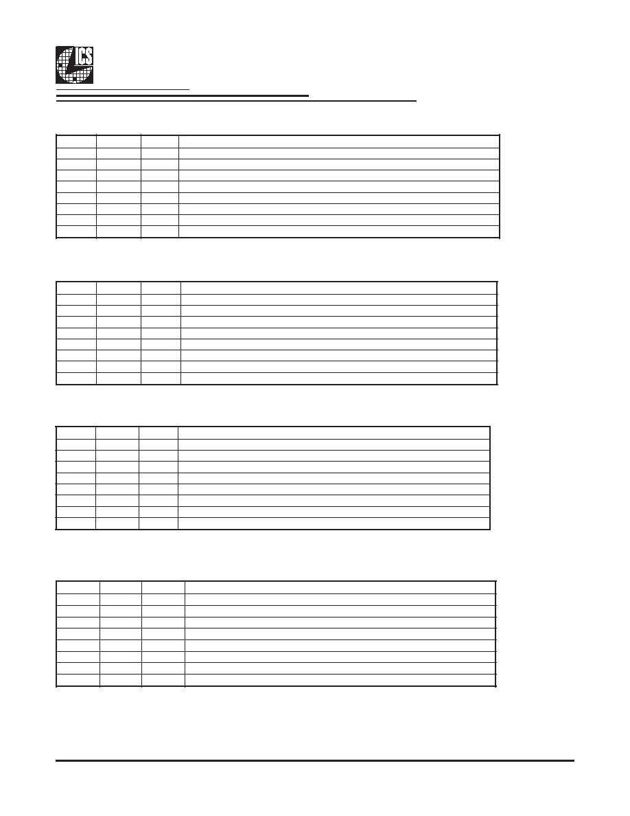
Byte 1: Output Control Register
(1 = enable, 0 = disable)
Byte 3: Output Control Register
(1 = enable, 0 = disable)
Byte 2: Output Control Register
(1 = enable, 0 = disable)
Byte 4: Output Control Register
(1 = enable, 0 = disable)
t
i
B#
n
i
PD
W
Pn
o
i
t
p
i
r
c
s
e
D
7
t
i
B4
4
,
5
41
2
C
/
T
U
P
C
6
t
i
B7
3
,
8
31
1
C
/
T
U
P
C
5
t
i
B0
4
,
1
41
0
C
/
T
U
P
C
4
t
i
B-
X
k
c
a
b
d
a
e
R
4
S
F
3
t
i
B-
X
k
c
a
b
d
a
e
R
3
S
F
2
t
i
B-
X
k
c
a
b
d
a
e
R
2
S
F
1
t
i
B-
X
k
c
a
b
d
a
e
R
1
S
F
0
t
i
B-
X
k
c
a
b
d
a
e
R
0
S
F
t
i
B#
n
i
PD
W
Pn
o
i
t
p
i
r
c
s
e
D
7
t
i
B-
1
d
e
v
r
e
s
e
R
6
t
i
B7
11
9
_
K
L
C
I
C
P
5
t
i
B6
11
8
_
K
L
C
I
C
P
4
t
i
B5
11
7
_
K
L
C
I
C
P
3
t
i
B4
11
6
_
K
L
C
I
C
P
2
t
i
B2
11
5
_
K
L
C
I
C
P
1
t
i
B1
11
4
_
K
L
C
I
C
P
0
t
i
B0
11
3
_
K
L
C
I
C
P
t
i
B#
n
i
PD
W
Pn
o
i
t
p
i
r
c
s
e
D
7
t
i
B-
X
)
k
c
a
b
d
a
e
r
(
0
L
E
S
i
t
l
u
M
6
t
i
B-
X
)
k
c
a
b
d
a
e
R
(
1
L
E
S
i
t
l
u
M
5
t
i
B1
31
0
_
6
V
3
4
t
i
B0
31
1
_
6
V
3
t
i
B8
41
0
F
E
R
2
t
i
B1
1
F
E
R
1
t
i
B7
21
z
H
M
8
4
_
6
V
3
0
t
i
B8
21
2
_
6
V
3
Notes:
1. PWD = Power on Default
2. For disabled clocks, they stop low for single ended clocks. Differential CPU clocks stop with CPUCLKT at high,
CPUCLKC off, and external resistor termination will bring CPUCLKC low.
t
i
B#
n
i
PD
W
Pn
o
i
t
p
i
r
c
s
e
D
7
t
i
B3
21
z
H
M
8
4
_
4
2
6
t
i
B2
21
z
H
M
8
4
5
t
i
B-
1
e
l
b
a
s
i
D
=
0
,
e
l
b
a
n
E
=
1
t
c
e
t
e
d
t
f
i
h
s
r
a
e
g
t
e
s
e
R
4
t
i
B-
0
I
=
1
;
e
r
a
w
d
r
a
h
y
b
#
4
2
_
8
4
l
e
S
=
0
2C
3
t
i
B-
0
z
H
M
8
4
=
1
,
z
H
M
4
2
=
0
,
#
4
2
_
8
4
l
e
S
2
t
i
B8
1
2
_
K
L
C
I
C
P
1
t
i
B7
1
_
K
L
C
I
C
P
0
t
i
B6
1
0
_
K
L
C
I
C
P
发布紧急采购,3分钟左右您将得到回复。
相关PDF资料
ICS950908BFLF
IC TIMING CTRL HUB P4 56-SSOP
ICS951402AGLF
IC TIMING CTRL HUB P4 48-TSSOP
ICS95V847AGIT
IC CLOCK DRIVER 2.5V 24-TSSOP
ICS95V850AGT
IC CLK DVR PLL 1:10 48TSSOP
ICS95V857ALT
IC CLK DVR PLL 1:10 40TVSOP
ICS95V857CKLF8
IC CLK DVR PLL 1:10 40VFQFN
ICS97U870AKT
IC CLK DVR PLL 1:10 40VFQFN
ICS97ULP877AHT
IC CLOCK DRIVER 1.8V LP 52-BGA
相关代理商/技术参数
ICS950218AFLF
功能描述:IC TIMING CTRL HUB P4 48-SSOP RoHS:是 类别:集成电路 (IC) >> 时钟/计时 - 专用 系列:TCH™ 标准包装:28 系列:- 类型:时钟/频率发生器 PLL:是 主要目的:Intel CPU 服务器 输入:时钟 输出:LVCMOS 电路数:1 比率 - 输入:输出:3:22 差分 - 输入:输出:无/是 频率 - 最大:400MHz 电源电压:3.135 V ~ 3.465 V 工作温度:0°C ~ 85°C 安装类型:表面贴装 封装/外壳:64-TFSOP (0.240",6.10mm 宽) 供应商设备封装:64-TSSOP 包装:管件
ICS950218AFLFT
功能描述:IC TIMING CTRL HUB P4 48-SSOP RoHS:是 类别:集成电路 (IC) >> 时钟/计时 - 专用 系列:TCH™ 标准包装:28 系列:- 类型:时钟/频率发生器 PLL:是 主要目的:Intel CPU 服务器 输入:时钟 输出:LVCMOS 电路数:1 比率 - 输入:输出:3:22 差分 - 输入:输出:无/是 频率 - 最大:400MHz 电源电压:3.135 V ~ 3.465 V 工作温度:0°C ~ 85°C 安装类型:表面贴装 封装/外壳:64-TFSOP (0.240",6.10mm 宽) 供应商设备封装:64-TSSOP 包装:管件
ICS950218AFT
功能描述:IC TIMING CTRL HUB P4 48-SSOP RoHS:否 类别:集成电路 (IC) >> 时钟/计时 - 专用 系列:TCH™ 标准包装:1,500 系列:- 类型:时钟缓冲器/驱动器 PLL:是 主要目的:- 输入:- 输出:- 电路数:- 比率 - 输入:输出:- 差分 - 输入:输出:- 频率 - 最大:- 电源电压:3.3V 工作温度:0°C ~ 70°C 安装类型:表面贴装 封装/外壳:28-SSOP(0.209",5.30mm 宽) 供应商设备封装:28-SSOP 包装:带卷 (TR) 其它名称:93786AFT
ICS950218YFLF-T
制造商:ICS 制造商全称:ICS 功能描述:Programmable Timing Control Hub TM for P4 TM
ICS950220
制造商:ICS 制造商全称:ICS 功能描述:Programmable Timing Control Hub⑩ for P4⑩
ICS950220AFLF
功能描述:IC TIMING CTRL HUB P4 48-SSOP RoHS:是 类别:集成电路 (IC) >> 时钟/计时 - 专用 系列:TCH™ 标准包装:28 系列:- 类型:时钟/频率发生器 PLL:是 主要目的:Intel CPU 服务器 输入:时钟 输出:LVCMOS 电路数:1 比率 - 输入:输出:3:22 差分 - 输入:输出:无/是 频率 - 最大:400MHz 电源电压:3.135 V ~ 3.465 V 工作温度:0°C ~ 85°C 安装类型:表面贴装 封装/外壳:64-TFSOP (0.240",6.10mm 宽) 供应商设备封装:64-TSSOP 包装:管件
ICS950220AFLFT
功能描述:IC TIMING CTRL HUB P4 48-SSOP RoHS:是 类别:集成电路 (IC) >> 时钟/计时 - 专用 系列:TCH™ 标准包装:28 系列:- 类型:时钟/频率发生器 PLL:是 主要目的:Intel CPU 服务器 输入:时钟 输出:LVCMOS 电路数:1 比率 - 输入:输出:3:22 差分 - 输入:输出:无/是 频率 - 最大:400MHz 电源电压:3.135 V ~ 3.465 V 工作温度:0°C ~ 85°C 安装类型:表面贴装 封装/外壳:64-TFSOP (0.240",6.10mm 宽) 供应商设备封装:64-TSSOP 包装:管件
ICS950220YFLFT
制造商:ICS 制造商全称:ICS 功能描述:Programmable Timing Control Hub⑩ for P4⑩